
Warning: this post has lots of technical discussion. If you’re not interested in the details, I suggest you skip straight to the last paragraph!
As an RF Engineer, I was interested to see what the RF path on the Futaba R3006SB looks like, since I had to open it anyway to replace the antennas. The picture below shows the top side of the R3006SB PCB, where the RF circuitry resides.
This photograph, and the others in this article, were taken with my children’s Celestron Handheld Digital Microscope Pro.
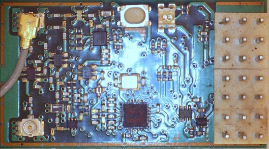
Futaba R3006SB PCB (top side)
The signal is routed from the antenna connectors on the left of the board to the IC between them, a uPG2214TB SPDT RF switch which selects which antenna to use.This is a fairly simple implementation of diversity, since only a single antenna can be used at any one time, and the choice of which antenna to use must be made in advance. While it does not exploit the two antennas to the fullest extent possible, it is appropriate for a simple, low-cost implementation.
The signal from the chosen antenna is routed to another uPG2214TB immediately to its right, which selects between the transmit path (towards the top of the PCB in the image) and the receive path (towards the bottom of the PCB).
Transmit Path
Although the R3006SB is described as a receiver, it is actually a transceiver, as it also transmits telemetry information. The transmit path leads via a filter to a uPG2301TQ RF power amplifier (the smaller square IC just below and to the left of the push-button switch), which provides a maximum power output of +23 dBm (200 mW). The input to the PA comes from another uPG2214TB switch, which allows either the transmit path or the receive path to be connected to the RF transceiver IC (large square package at the bottom centre of the PCB).
Receive Path
The receive signal is routed from the TX/RX switch, via a filter to an IC that I have not been able to conclusively identify (see below). The marking appears to be “02 41U”.
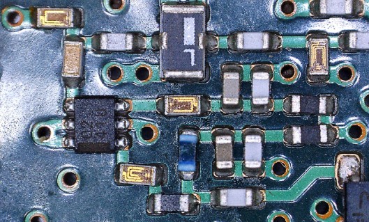
Unidentified IC and Associated Circuitry
This looks like a two-stage LNA, with the input on pin 4 (top left n the image above), output on pin 1 (bottom right) and the decoupled supply voltage applied both to the output (pin 1) through an RF choke (the blue component) and to pin 3 through matching inductors. This is a very unusual pin-out for an LNA, and I spent many hours searching for a possible candidate.
The only candidate I found is the New Japan Radio NJG1130KA1. This has the same unusual pin-out, the same package marking (with “02” being the smd marking code and “41U” the date code and manufacturing batch number), and the package shape and size (1.6mm x 1.2mm) is correct within my measurement error. The application circuit from the datasheet (see below) also very similar to the circuit on the PCB, although I have not verified component values. Note that the dotted near the bottom of the IC symbol indicates the location of the pin 1 indicator, which confirms that the orientation is the same as on the PCB. The only significant changes are the addition of a series matching inductor at the output, and a change to the matching circuit at the input of the device, which might both be due to the operating frequency (see below).
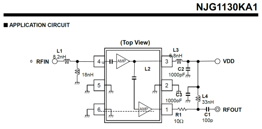
The only difficulty with this identification is that the NJG1130KA1 is intended as an LNA for GPS receivers, and is specified for operation at 1.575GHz, not in the 2.4GHz ISM band. It is possible that NJR developed a specific tuning solution to allow Futaba to use this LNA in the 2.4GHz band, which would account for the additional matching components, but I couldn’t find an application note that confirms this. Alternatively, there may be a derivative of this LNA that is designed for operation at 2.4 GHz, but I have not been able to find such a device.
When operated at 1.575 GHz the NJC1130KA1 is specified for 20 dB gain with a noise figure of 0.65 dB and 1 dB compression at +11 dBm output. I would expect the gain to be somewhat reduced at 2.4 GHz.
Postscript: when reviewing the SF800 S-FHSS receiver, I found that it has a very similar circuit and the markings on the corresponding IC \identified it as a UA2725 Low Noise Amplifier (LNA) with a gain of 20 dB and noise figure of 1.9 dB at 2.4 GHz. I expect that the R3008SB uses a similar (or identical) LNA.
RF Transceiver
Some attempt seemed to have been made to obscure the identity of the RF Transceiver IC, which is that large square IC at the centre bottom of the first image, with some scratching of the surface and a blob of red paint. However a bit of cleaning with mineral turpentine left it easily identifiable…
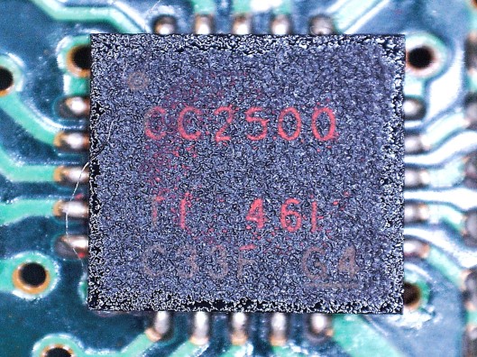
TI CC2500 RF Transceiver
It’s a Texas Instruments CC2500, described by its datasheet as a “Low-Cost Low-Power 2.4 GHz RF Transceiver”. It supports frequency-hopping and frequency-shift keying (FSK) modulation with symbol rates from 1.2 to 500 kBaud. This shows that the Futaba T-FHSS system uses Frequency Shift Keying (FSK) modulation, rather than the more bandwidth- and power-efficient Phase Shift Keying (PSK). This is not surprising since FSK is simpler (and thus cheaper) to implement than PSK, and T-FHSS is Futaba’s “low-cost” option.
The output power is programmable up to +1 dBm, which would be sufficient to drive the UPG2301TQ RF power amplifier to generate about +22dBm output. Allowing for filtering losses, this suggests a maximum transmit power of about +20 dBm (100 mW) at the antenna port.
Conclusion
The R3006SB has clearly been designed for simplicity and low cost – this is apparent from the the simple implementation of antenna diversity and the use of frequency-shift keying. In my opinion, superior performance could be obtained by a more sophisticated diversity scheme in conjunction with PSK modulation and source coding to reduce the data rate. However this would have increased the complexity and cost of the system, so the design is appropriate to its place as the low cost option in the Futaba RC ecosystem. Taking this into account, the receiver RF architecture appears to have been well engineered to meet its requirements.

Pingback: Futaba S-FHSS Protocol Overview | RF Eng FPV
Pingback: KS-Servo SF800 S-FHSS Receiver Review | RF Eng FPV